For my second co-op position in 2019, I took up a research position at the University of Wurzburg – one of the oldest universities in Germany.
This was to be a series of firsts: my first time going to Europe, my first time living alone, and my first time in a research position.
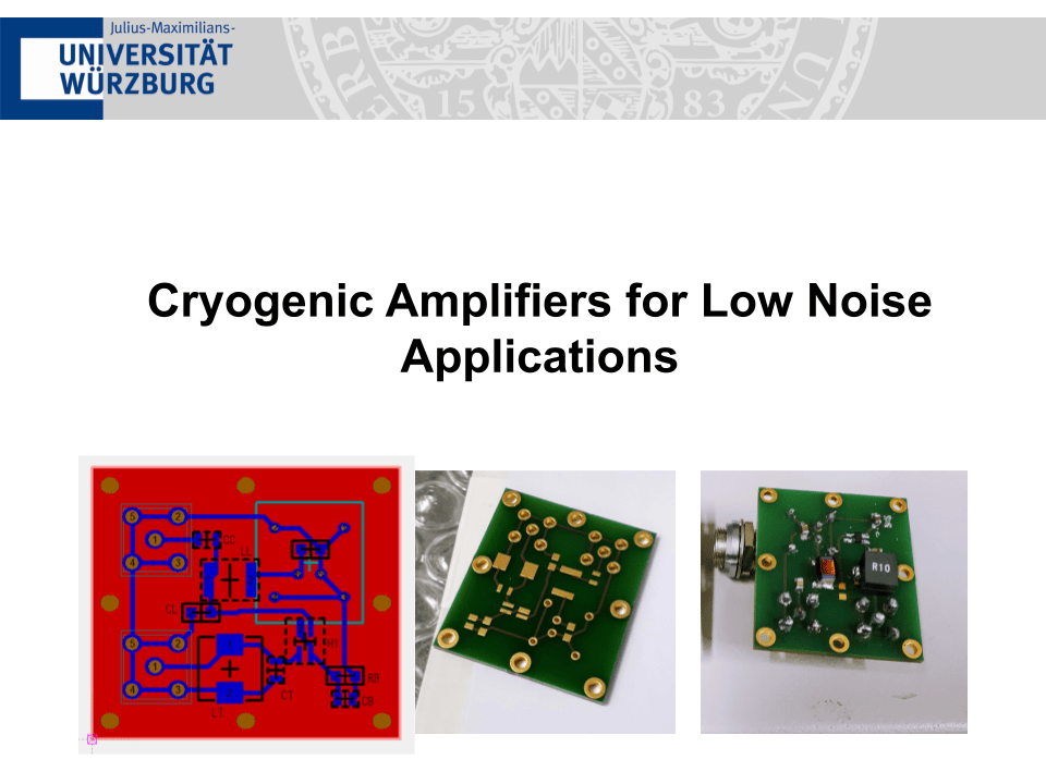
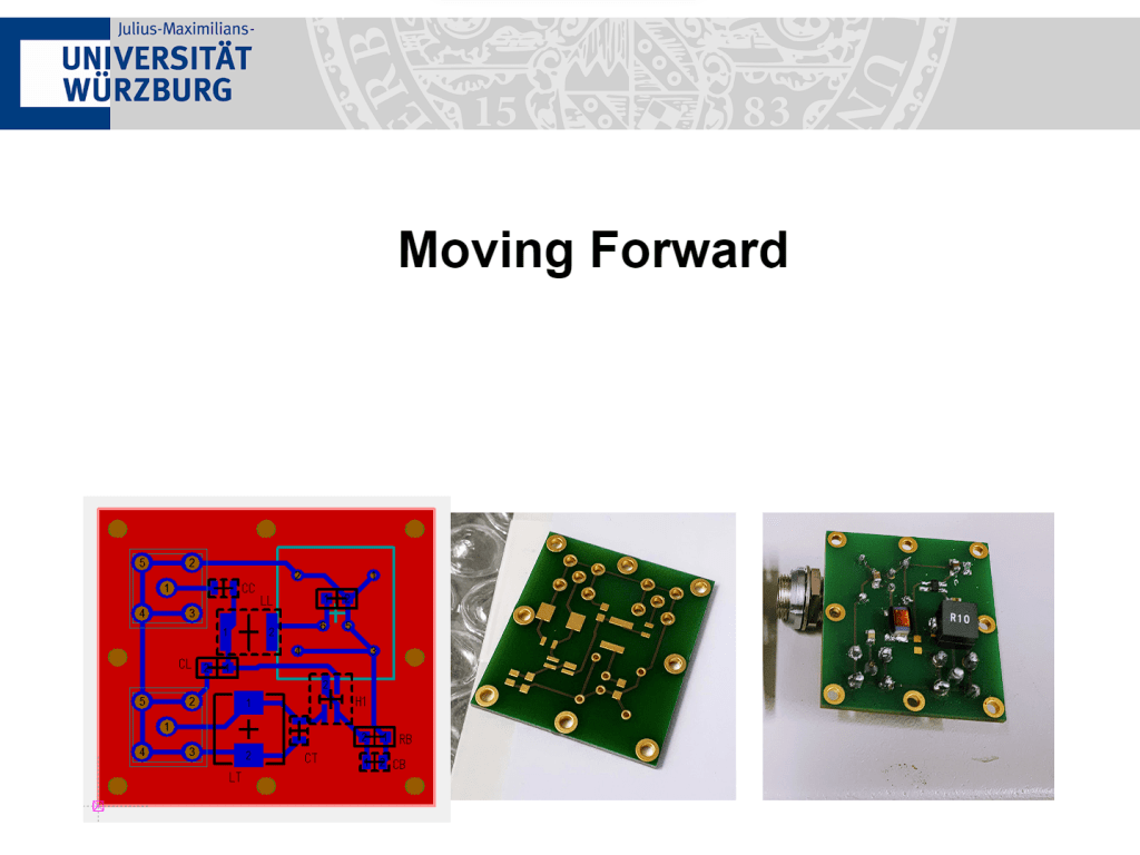
Eight months sounded short on paper, but a lot can be done in that amount of time. In eight months I went from a very basic understanding about electronics to designing circuit boards for measurements at under five Kelvin (5K = -268.15°C).
cryogenic circuits – background
There’s only a few reasons for cooling down circuits to such low temperatures. There are some interesting physics that happens at these temperatures – superconductivity for one. But another important reason is that you eliminate a source of noise: Johnson-Nyquist noise (aka thermal noise). This is huge when your goal is to read the tiniest of signals. In my case, the goal was to measure electron temperature.
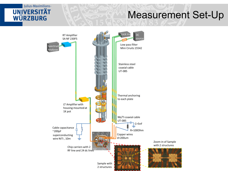
The samples are shown in the zoomed in photo on the bottom right. This entire system is contained within a dilution refrigerator save for the boxes at the ends of the green cables. In order to read the signal output on the spectrum analyzer the signal needs to be amplified by quite a bit. It is not enough to just increase the input signal since, as mentioned, the amount of noise will increase significantly. Using just a single amplifier at room temperature (pictured in blue) is subject to losses along the cable resulting in a low signal-to-noise ratio. Introducing a second amplifier within the fridge that is kept also at low temperatures will help to amplify the signal enough so that the losses along the rest of the cable become negligible.
noise
There are 3 main types of noise of concern that I will bring up that are important at low temperatures:
- Johnson-Nyquist Noise, “thermal noise”- as mentioned above, this is thermal noise that is inherent from the motion of electrons. It does not change with frequency.
- Shot Noise: this is generated by the random arrival of charge carriers. It is proportional to current and bandwidth.
- 1/f noise, “pink noise”: This is a type of noise that decreases frequency. It can arise from things such as surface defects.
amplifier features
There are many amplifier features that are important for design. The main ones that were of concern for this design were the frequency response, power consumption, and input impedance.
Power Consumption: For noise reasons, power consumption is desired to be as low as possible. Simply put, more power = more heat generated = more thermal noise.
Input Referred Noise: Ideally the noise generated by the circuit itself is smaller than the signal that we want to measure. This becomes hugely important as we are measuring signals on the scale of a single electron. Making sure that all the noise sources listed above are reduced as much as possible is important for maximizing our signal-to-noise ratio.
Input Impedance: Having a higher input impedance would greatly increase the signal-to-noise ratio. If it is too low then we can have some negative effects on the signal voltage as the input will act as a resistor divider.
benchmarks
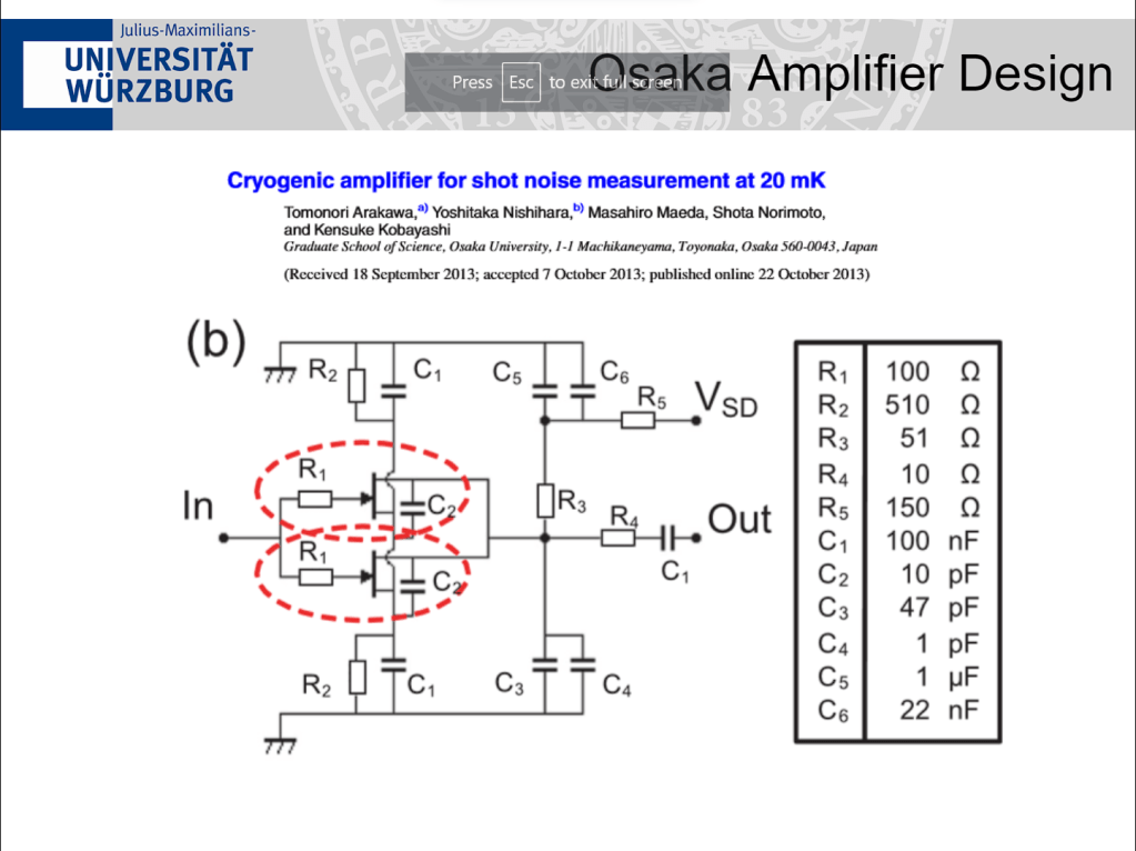
There are two amplifier designs which we were benchmarking against to evaluate the performance of our device. The first comes from a paper published from Osaka University by Arakawa et al. The main feature of this design is the use of two High-Electron Mobility Transistors (HEMTs) in parallel. Here they are able to show that this reduces the 1/f noise that is inherent from the HEMTs. The design also uses a lot of passive components for filtering and adjusting the frequency response. The one drawback is that the increased number of components increases the overall thermal noise.
The second design we benchmark against comes from a research group at Weizmann Institute of Science located in Rehovot, Israel. A very similar approach is taken but with much fewer passive components. I do not have a schematic for this but the important point is that it is slightly better than what you see above.
design
Now we finally come to the chosen design.
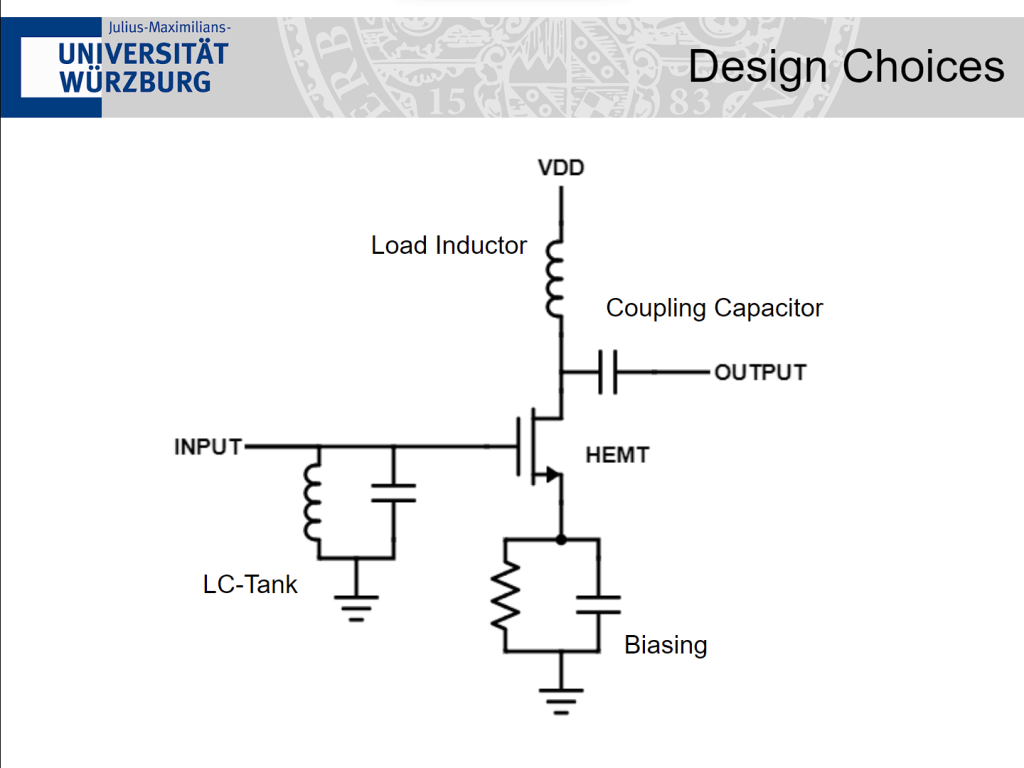
They simple is better and I have to agree. The main goal with this design is to reduce the number of passive components as much as possible. The circuit can be divided into 4 main parts, each with 1 or 2 components.
First, the LC tank is used to adjust our bandwidth based on our measurement.
The HEMT is biased using a resistor and capacitor in parallel to set the DC operating point of the HEMT. This is important so that it behaves properly in a way which we expect. And a HEMT is chosen specifically for it’s excellent charge carrier mobility characteristics thus producing less noise.
The coupling capacitor gets rid of DC voltage at the output.
And the load inductor is used to convert the sourced current from the HEMT into a voltage. Typically a resistor is used for this but the gambit was that having an inductor would reduce the thermal noise produced overall by the circuit (from having one less resistor) but it carries some concern. The main concern was a self-resonance with the capacitor in the biasing circuit which could be a source of noise within our bandwidth.
challenges
Surprisingly, the main challenge that arose came from the input part of the circuit. The inductor in the LC tank that is used for selecting our bandwidth is typically pretty large (on the order of ~10uH). One issue with larger inductors is the series resistance that they inherit. This has the effect of both creating more thermal noise and decreasing the input impedance of the circuit.
The other challenge comes from our cable capacitance. The small capacitance from the shielded cables that I used for testing were enough to shift the frequency response by a significant amount. The LC tank values have to be adjusted to compensate for this shift due to cabling as well.
results
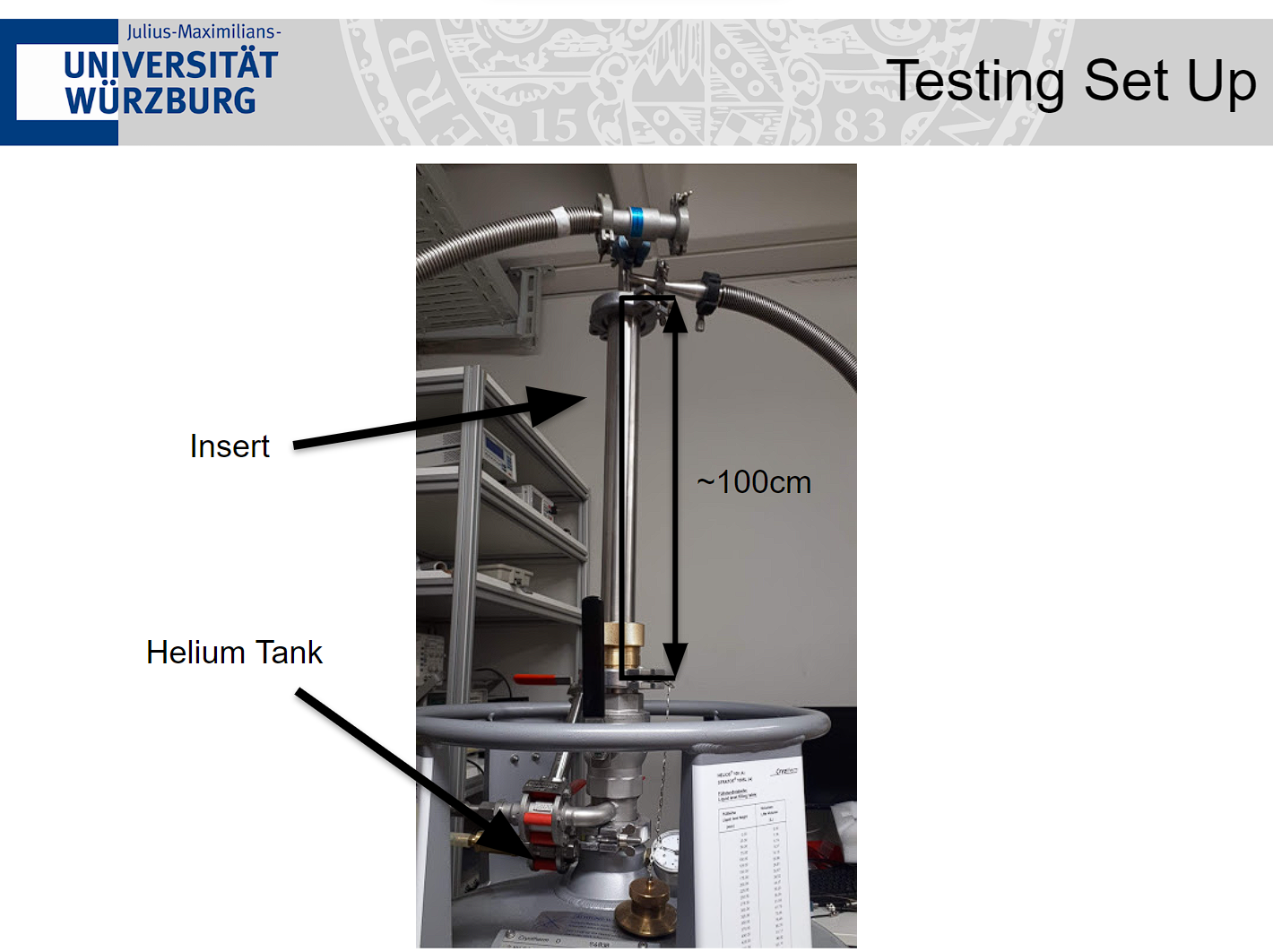
The set up for testing is shown above. The circuit was sealed into a giant metal insert which would have the air pumped out. The entire metal tube would then be lowered very slowly into a tank of liquid Helium. The lack of air in the tube will make it so that there will be no condensation which could cause issues in the circuit. The tube is lowered slowly so that there isn’t a thermal shock which would both build up pressure in the Helium tank as the liquid evaporates, and to evenly cool the insert so it will not wear down. The whole process takes about an hour of careful work (sometimes just to realize that the cables stopped working because something shifted when you seal the tube).
Measurements are taken at both room temperature and at ~5K (liquid Helium is 4.2K).
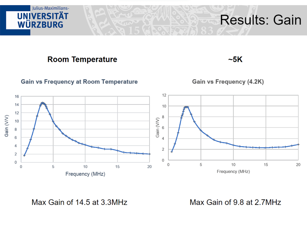
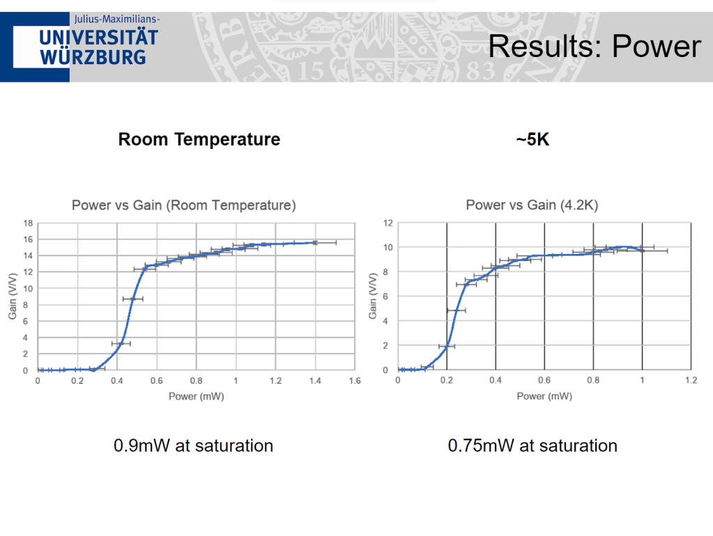
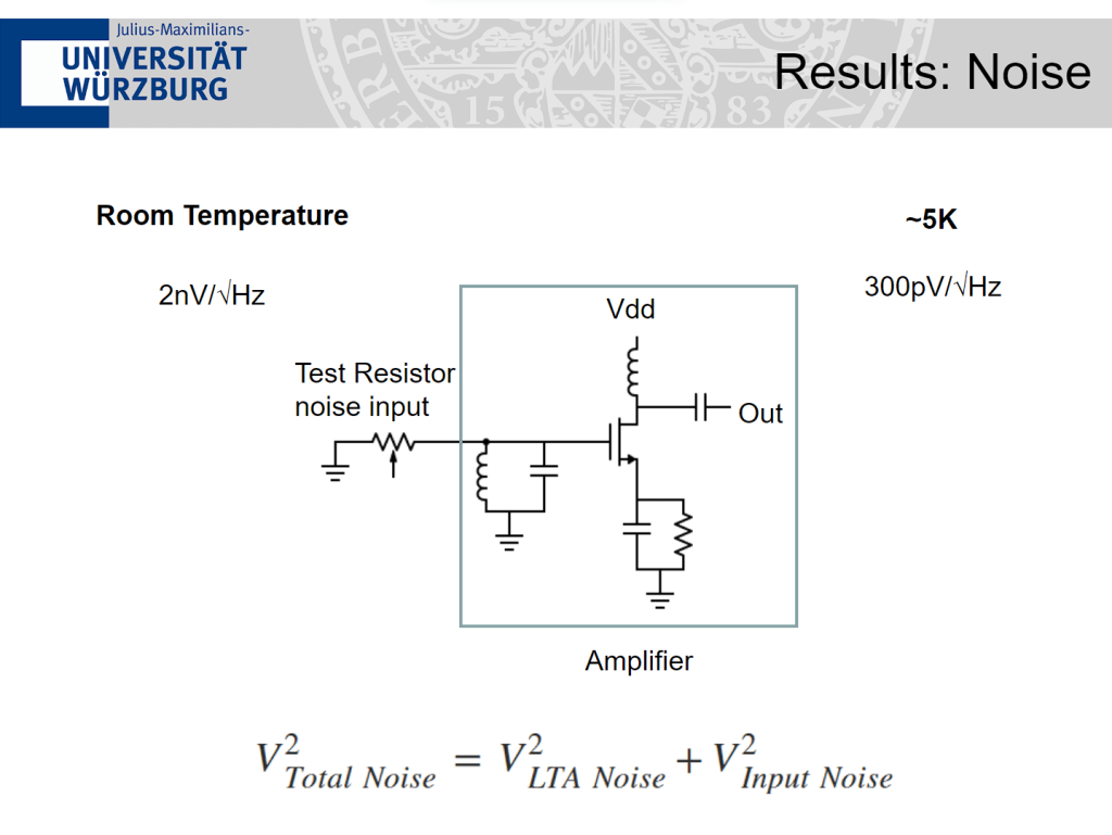
In summary, when going from room temperature to ~5K, the gain is reduced by about 33% but still workable, power consumption is reduced by 17%, and input referred noise is reduced by 85%.
But how does this compare to our benchmarks?

Our gain is comparable to the other published circuits (we expect that it would decrease slightly as we get to lower temperatures) but our power consumption is much lower than the field, partly to do with using a load inductor in place of a load resistor. The input referred noise is on par but we also expect that to decrease as we get to lower temperatures.
closing remarks
Throughout this co-op I was able to experience the highs and low of academic research. The frustration of wasting time on measurements which all turn out to be garbage because of a rogue cable and thinking “maybe none of this actually works”. The skepticism that what you see isn’t real so you do the measurement 5 more times, just to be sure. And getting results that are decent but not as good as you expect but it’s fine because you can always blame “parasitics”.
Overall, my time in Germany was a great adventure. I’ve learned a lot about circuits at a very fundamental level, designed my first ever PCBs, assembled my first ever PCBs, and enjoyed the European heat wave with my cool cool circuits.
